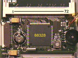
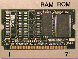
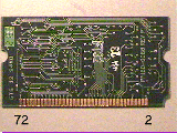
3. My conventions:
3.1 Memory module and its connector
- 72 pins, from 1 to 72. Pin 1 is the leftmost pin at component side. Odd pins on the
component side and, of course, even pins on the other side. This way, pin 71 is the
rightmost on the component side.
Look at memory schematics for a table of memory pinouts.
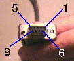
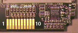
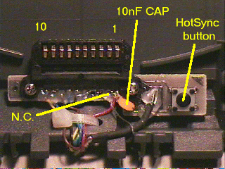
3.2 Cradle & Pilot external connectors
- 10 pins, from 1 to 10. Pin 1 is the rightmost pin when facing the cradle.
Pin 1 is also the leftmost pin when facing the back of Pilot.
- The DB9F connector has 9 pins, from 1 to 9. Take a look at following pictures:
[ Next Page ] [ Previous Page ] [ Main Page ]